Fitting
The Fitting tab is where equivalent circuits can be fitted to data sets (Fig. 20):
the various settings that determine how the fitting is performed
combo boxes that can be used to choose the active data set, the active fit result, and the active output
a table of fitted parameter values and estimated errors (if possible to estimate)
a table of statistics related to the active fit result
a table of the settings that were used to obtain the active result
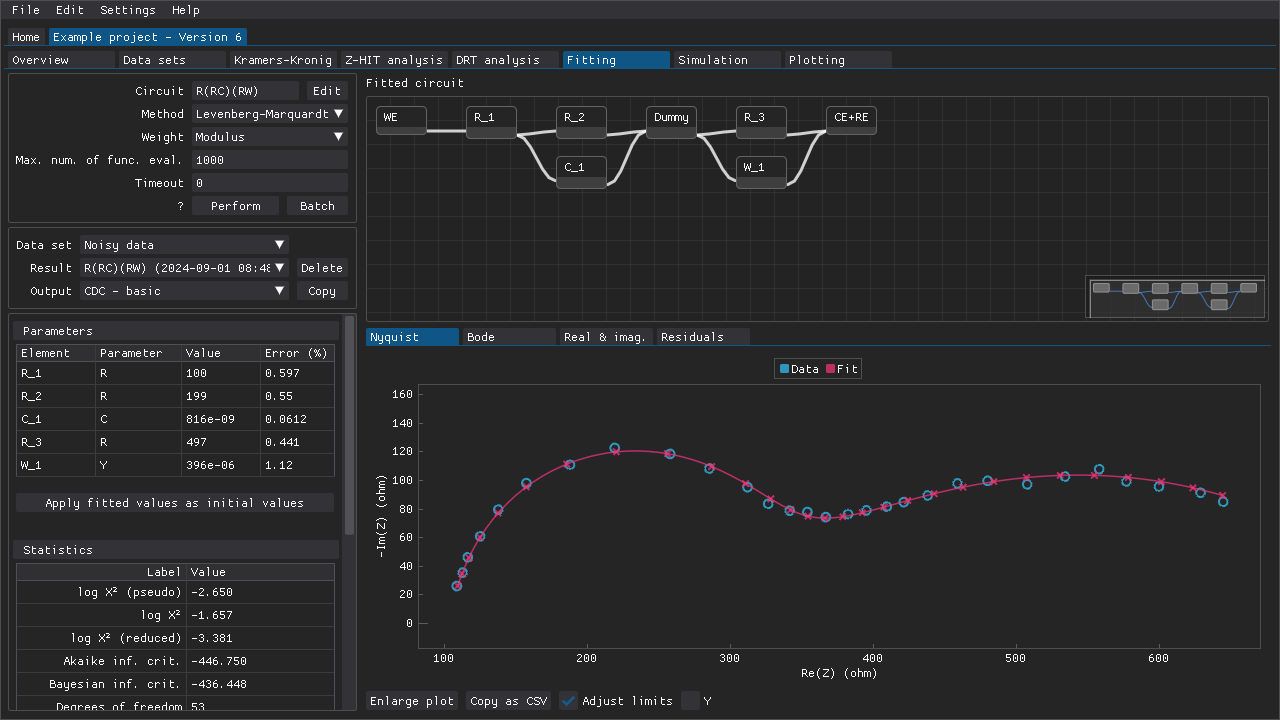
Fig. 20 An example of an R(RC)(RW) circuit that has been fitted to a data set. The obtained fitted parameters are close to the parameters that were used to generate the data set in the first place.
Equivalent circuits can be constructed either by typing in a corresponding circuit description code (CDC) or by using the graphical circuit editor, which is accessible by pressing the Edit button.
Different iterative methods and weights are available. If one or both of these settings are set to Auto, then combinations of iterative method(s) and weight(s) are used to perform multiple fits in parallel and the best fit is returned.
The results are presented in the form of a table containing the fitted parameter values (and, if possible, error estimates for the fitted parameter values), a table containing statistics pertaining to the quality of the fit, three plots (Nyquist, Bode, and relative errors of the fit), and a preview of the circuit that was fitted to the data set. If you hover the mouse cursor over the cells in the tables, then you can get additional information (e.g., more precise values or explanations).
Note
It may not always be possible to estimate errors for fitted parameters. Common causes include:
A parameter’s fitted value is close to the parameter’s lower or upper limit.
An inappropriate equivalent circuit has been chosen.
The maximum number of function evaluations is set too low.
The data contains no noise and the equivalent circuit is very good at reproducing the data.
Equivalent circuits
The CDC syntax is quite simple:
Circuit elements are represented by one or more letter symbols such as
Rfor a resistor,Cfor a capacitor, andWofor a Warburg diffusion of finite-length with a reflective boundary.Two or more circuit elements enclosed in parentheses,
(), are connected in parallel.Two or more circuit elements enclosed in square brackets,
[], are connected in series. This can be used to construct, e.g., a parallel connection that contains a nested series connection ((C[RW])whereRandWare connected together in series and that series connection is in parallel withC).
DearEIS also supports an extended CDC syntax.
This extended syntax allows for defining circuit elements with, e.g., labels, initial values for parameters, and parameter limits.
Circuit elements can be followed up by curly braces and the aforementioned things can be defined within these curly braces.
For example, R{R=250f:ct} defines a resistor with:
an initial value of 250 ohms for the resistance
Ra fixed initial value (i.e., a constant value)
the label
ct, which stands for charge transfer
E notation (e.g., 1e-6 or 1E-6 instead of 0.000001) is supported by the extended syntax.
All parameters do not need to be defined if a circuit element has multiple parameters.
If parameters are omitted, then the default values are used (e.g., the default initial value for the R parameter of a resistor is 1000 ohms).
If parameter limits are completely omitted, then the default values are used (e.g., the default lower limit for the R parameter of a resistor i 0 and the upper limit is infinity).
Q{Y=1.3e-7//1e-5,n=0.95/0.9/1.0:dl} defines a constant phase element with:
an initial value of 1.3 * 10^-7 F*s^(n-1) for the
Yparameter (other sources may use the notationAorQ0for this parameter) with no lower limit and an upper limit of 1 * 10^-5 F*s^(n-1)an initial value of 0.95 for the
nparameter (other sources may use the notationalphaorpsifor this parameter) with a lower limit of 0.9 and an upper limit of 1.0the label
dl, which stands for double-layer (i.e., double-layer capacitance)
The valid symbols are listed in the Elements tab found within the Diagram tab of the Circuit editor window.
Alternatively, nodes representing the circuit elements can be added to the node editor and connected together to form an equivalent circuit. Circuit elements can be added to the node editor by clicking on a type of element in the Elements tab or by dragging a type of element from the Elements tab and onto the node editor. The nodes can be linked together by clicking and dragging between the terminals of the nodes (i.e., the yellow dots on either side of a node). If two parallel circuits are connected in series like in Fig. 21, then it is necessary to place a node between them. This node could be an element (e.g., a resistor) that is also connected in series to the two parallel circuits or it could be a dummy node. This dummy node, which can be added with the Add dummy/junction button, does not affect the impedance of the system at all. Links between nodes can be deleted by either clicking on a link and then pressing the Delete button on the keyboard, or by holding down Ctrl when clicking on a link. Multiple nodes can be moved or deleted by clicking and dragging a selection box around them.
Note
Click and hold on a terminal/pin (yellow dot) to start creating a link and then drag and release near another terminal/pin. Hold down Ctrl while clicking on a link to remove the link.
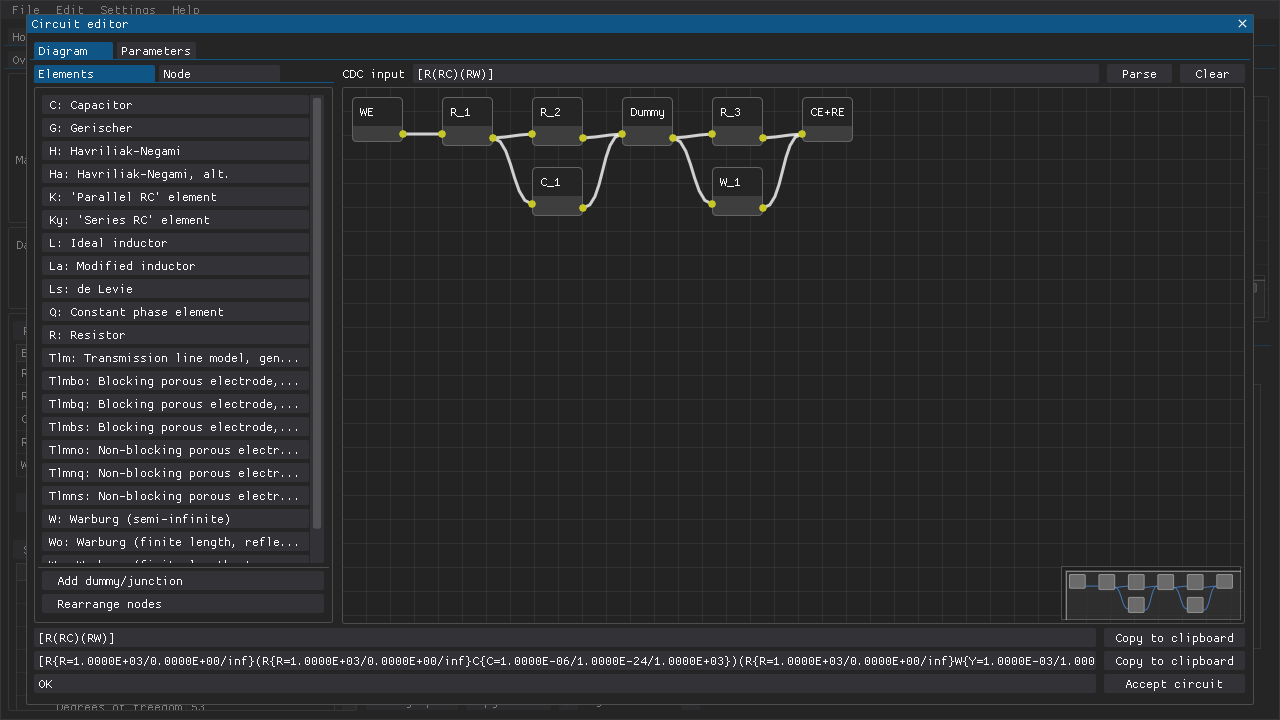
Fig. 21 The graphical circuit editor can be used to construct equivalent circuits and to define the initial values and limits of parameters.
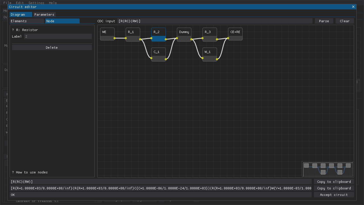
Fig. 22 Selecting a node makes it possible to assign a label (e.g., ct for charge transfer).
Note
Due to technical reasons, one must click on the upper part of a node (i.e., where the label is) that represents a circuit element in order to be able to define, e.g., custom initial values.
Also, any values typed into the input fields must be confirmed by pressing Enter or the value will not actually be set.
Click and hold on the lower part of the node to move it around.
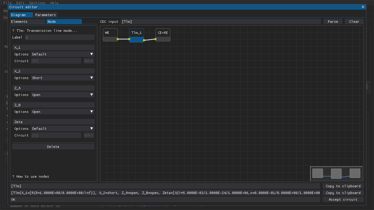
Fig. 23 Container elements such as the general transmission line model have subcircuits that can also be modified.
Press the Accept circuit button in the bottom right-hand corner once the equivalent circuit is complete. If there is an issue with the equivalent circuit (e.g., a missing or invalid connection), then the button will be labeled Cancel instead. The Status field at the bottom of the window should offer some help regarding the nature of the issue and the affected node should be highlighted with a red label (Fig. 24).
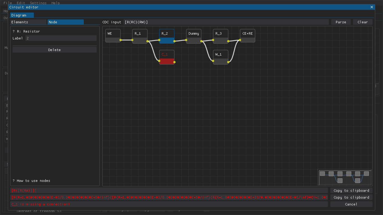
Fig. 24 If the circuit is invalid because of, e.g., a missing connection, then that is indicated by highlighting the affected node and by showing a relevant error message in the status field near the bottom of the window.
Adjusting parameters
The initial values of the parameters of each circuit element can be adjusted via the circuit editor’s Parameters tab. This tab provides a real-time preview of the impedance/admittance spectrum produced by the circuit. The lower and/or upper limits of the parameters can also be defined, and parameters can also be given fixed values.
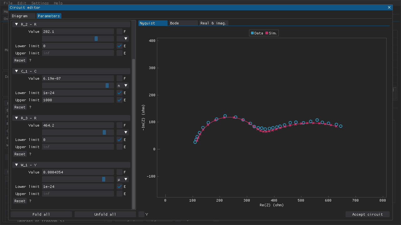
Fig. 25 The Parameters tab of the Circuit editor window provides a convenient way of dialing in the initial values before performing a fit.
It is possible to apply the values, which were obtained by fitting a circuit, as the initial values for another iteration of circuit fitting. This is accomplished by clicking the Apply fitted values as initial values button that can be found below the table of fitted values in the Fitting tab of the project.
Applying old settings and masks
The settings that were used to perform the active fitting result are also presented as a table and these settings can be applied by pressing the Apply settings button.
The mask that was applied to the data set when the fitting was performed can be applied by pressing the Apply mask button. If the mask that is applied to the data set has changed since an earlier fitting was performed, then that will be indicated clearly above the statistics table.
These features make it easy to restore old settings/masks in case, e.g., DearEIS has been closed and relaunched, or after trying out different settings.
Copying results to the clipboard
Different aspects of the results can be copied to the clipboard in different plain-text formats via the Output combo box and the Copy button. For example, the following results can be copied:
the basic or extended CDC of the fitted circuit
a table of the impedance response of the fitted circuit as character-separated values
a table of the fitted parameters as, e.g., character-separated values.
a circuit diagram of the fitted circuit as, e.g., LaTeX or Scalable Vector Graphics (see example below)
the SymPy expression describing the impedance of the fitted circuit
Note
Variables in SymPy expressions use a different set of lower indices to avoid conflicting variable names. See Generating equations for more information.

Fig. 26 Example of a circuit diagram as it would look if it was copied as Scalable Vector Graphics.